Samsung and SK Hynix Race Toward Hybrid Bonding for Next-Gen HBM
Samsung Electronics and SK Hynix are contemplating the adoption of hybrid bonding technology for future generations of high-bandwidth memory (HBM). This shift is anticipated to significantly alter the landscape of the worldwide semiconductor equipment supply chain.
Hybrid bonding attaches DRAM chips within HBM stacks without employing "bumps," but rather through copper-to-copper direct bonding. This method allows for a smaller chip footprint while significantly increasing both power efficiency and overall performance beyond double.
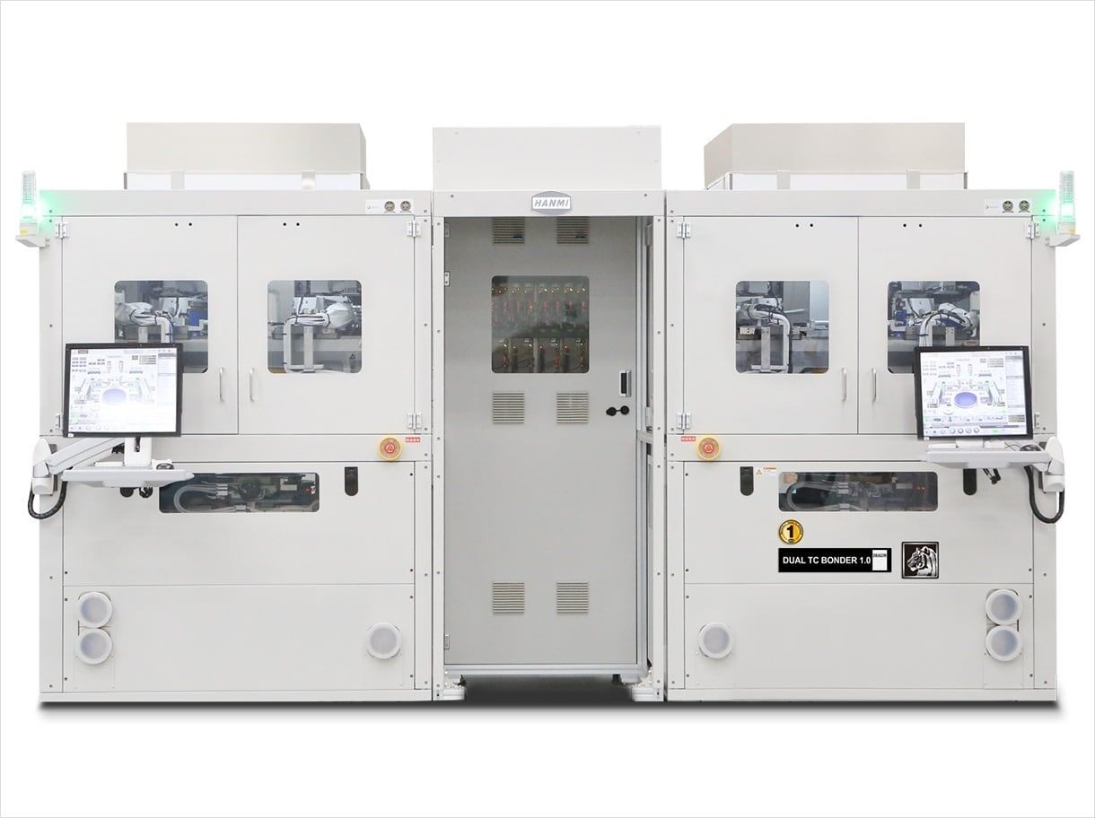
Earlier, high-bandwidth memory (HBM) manufacturing primarily used thermocompression (TC) bonder machines supplied by companies like SEMES, Hanmi Semiconductor, and Hanwha Semitek. Nevertheless, so far, no South Korean firm has achieved large-scale production using hybrid bonding technology. With the American semiconductor equipment leader Applied Materials announcing its move into the hybrid bonding sector for HBMs, a significant competitive battle looms ahead regarding control of the future supply chain.
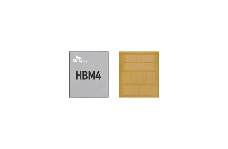
On May 7, according to information from industry insiders, both Samsung Electronics and SK hynix are developing plans to integrate hybrid bonding into the large-scale manufacturing processes of their upcoming advanced HBM models. It appears that Samsung could be incorporating this technology into its sixth-generation High Bandwidth Memory product, referred to as HBM4, possibly starting next year. Meanwhile, SK hynix seems poised to utilize hybrid bonding in what they call the seventh-generation version of their memory solution, labeled HBM4E.
At present, TC bonder machines are utilized for producing the most recent HBM3E (the fifth iteration of High Bandwidth Memory) components. These systems use both heat and force to join separate DRAM chips together, arranging them in layers with consistent spacing through bump interconnections. For their TC bonding machinery needs, Samsung mainly turns to suppliers like SEMES and Japan’s SHINKAWA Electric. In contrast, SK hynix predominantly depends on Hanmi Semiconductor and Hanwha Semitek for these requirements. Meanwhile, American company Micron Technology, who provides HBM modules to Nvidia, acquires its bonding apparatuses from Hanmi Semiconductor as well as Shinkawa.
Although SHINKAWA Electric and ASMPT from Singapore provide TC bonders to worldwide memory chip producers, South Korean companies lead this sector with more than 80 percent of the global share. In the realm of HBM3E TC bonders, Hanmi Semiconductor virtually controls the market.
It is anticipated that Hanwha Semitek will provide a significant number of the TC bonding tools for SK hynix’s 12-layer HBM3E manufacturing, starting from the second quarter. Additionally, SEMES equipment is extensively used across Samsung’s HBM fabrication lines.
The rise in demand for HBM has resulted in a significant uptick in TC bonder orders from local companies such as Hanmi Semiconductor," stated an official from the semiconductor equipment industry. "In order to fulfill agreements promptly, purchasers usually opt to place their orders with vendors that possess reliable large-scale manufacturing abilities.
As the market for hybrid bonding starts to grow, this transition is expected to cause significant disruption throughout the world of semiconductor equipment. Upon adoption, the novel bonding technique may well become the predominant approach for assembling upcoming HBM devices.
Applied Materials has made a significant move by purchasing a 9 percent share in Besi, the sole global provider of specialized adhesion equipment needed for hybrid bonding technology. Additionally, Applied Materials has started delivering hybrid bonding tools to the systemic semiconductor industry ahead of widespread use.
Companies from South Korea, HANMI Semiconductor and Hanwha Semitech, are rapidly advancing the creation of cutting-edge stacking machinery designed for future generations. Besides working on hybrid bonding tools, these enterprises are also investing in fluxless bonding technologies with the aim of enhancing their market position. Although fluxless bonding may be simpler technologically compared to hybrid bonding processes, it has the advantage of not requiring flux—a substance usually used to help align chips and remove oxides—which ultimately enables smaller chip designs. It’s worth noting that Micron is currently considering this new approach for potential integration into their upcoming High Bandwidth Memory (HBM) stacking procedures.